When Intel first unveiled its 14nm process, the company made aggressive claims about its performance and power consumption. The delays and fab cancellations that followed took a great deal of wind out of its sails, leaving us to wonder if the 14nm delays would push back the entire product stack. Now Intel is striking back against its naysayers — today, the company has released an enormous amount of information on its upcoming Broadwell Y product, the laptop- and tablet-oriented Core M. Let’s dive into Core M, and also take a look at what it might mean for the desktop Broadwell chips that will surely follow.

Everything but the kitchen sink
According to Intel, it’s rearchitected nearly everything about the Core M in order to hit its aggressive power and performance targets. The memory controller, L1/L2 caches, I/O, PCI Express interface, and even the chip’s packaging have all been overhauled.
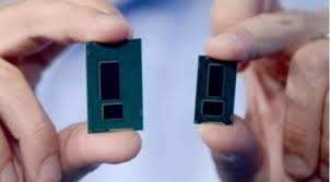
The Core M (codenamed Broadwell Y) will debut on Intel’s low-power 14nm process variant, which helps account for the chip’s dramatically improved power consumption — Intel argues it can deliver a greater-than 2x TDP improvement, 50% smaller packaging, a 25% physically smaller board, and a 60% reduction in SoC idle.
Intel is also claiming that Broadwell Y’s SRAM scaled to 58% its 22nm size when built on 14nm. That’s particularly impressive because it cuts against what other foundries are expected to deliver. Compare these claims below against what’s expected for the mainstream foundries like Samsung and GlobalFoundries (Intel first).